
READ THIS GUIDE THOROUGHLY AND REFER TO IT OFTEN!
Watch this tutorial by KK, a TA from the first offering of this course, on using Jade:
Watch the tutorial a second time while building the circuit here.
GENERAL OVERVIEW of JADE
Jade provides a framework for creating and simulating hierarchical block diagrams, including the digital logic circuits that we will design in this course.
The basic building block is a module. Each module has one or more aspects, which can be edited using one of the supplied editing tools. Currently Jade has editors for the following aspects:
schematic. A circuit diagram incorporating components (instances of other modules) with wires that run between the component terminals. Basic components (ground, vdd, ports, jumpers, text) are available on the toolbar; other components from the loaded module collections are available in the parts bin. The toolbar also has icons for simulation.
icon. When a schematic contains an instance of a module as a component, what appears in the diagram is the module's icon, usually a simple shape representing the component's functionality along with terminals that allow connections to be made to the component's ports.
properties. Modules have properties (key:value pairs) that further specify the behavior of a module, e.g., the memory module has a "contents" property specifying its contents. Properties have default values, which can be overridden for each instance of the module.
test. The test tool runs a simulation, providing a sequence of values for module's inputs and verifying that the expected values appear on the module's outputs. The test aspect provides the information needed to run the test.
JADE QUICK START GUIDE
- Tool tips, etc., appear in the status bar below the diagram
- The module tool bar appears at the top of the Jade window:
The module tools let you select an existing module to edit, create a new module (), make a copy of the current module under a new name (), delete the current module (), save all the user's modules to the module clipboard (), or select previously saved modules to load from the module clipboard to the current workspace ().

Module names look like file pathnames (/x/y/z) where the hierarchy is used to display the parts bin in an organized way. - To add a component to the schematic, click on the component in the parts bin and drag it into the schematic.
- Click to select a component, shift-click to add or remove a component from the current selection. You can also click on the schematic background, then drag out a selection rectangle which will select any component that intersects the rectangle.
- You can move selected components by clicking and dragging them to a new location.
- Delete selected components by typing DEL.
- There's a clipboard, accessible via , , , which operate on the currently selected components. The standard keyboard shortcuts of ctrl/cmd X, C, and V also work.
- Rotate/flip selected components using , , ,
- Double-click a component to edit its properties.
- Add wires by clicking on the open circle at component terminals or ends of wires, drag to create a wire.
- You can associate a signal name with a wire either by connecting it to a named port component or by double-clicking the wire and editing its name property. Wires with the same signal name are considered electrically connected. Wires have a width, either inferred from the signal name (e.g., "DATA[31:0]") or entered explicitly by editing the wire's Width property. The default width of a wire is 1.
A wire can represent a multi-bit numeric constant by giving it a name of the form number'width, where number can be in decimal (e.g., 10), binary (0b1010), or hex (0xA); the width in bits is always specified in decimal. For example, "5'4" would specify a wire of width 4, where the component signals are connected to gnd, vdd, gnd, vdd. - There is undo/redo support using , .
- You can pan and zoom the schematic or icon diagrams using the navigation controls in the upper left of the diagram. Zooming is helpful to verify connections of wires to components, which can be difficult to see with the default window size. You can also shift-click-and-drag on the diagram background to pan the diagram using the mouse.
JADE PROBLEMS AND SOLUTIONS
- Some common troubles with Jade stem from some inconsistencies in saving and loading circuits. Jade stores your designs in your browser's local storage, and some browsers handle this better than others. If you cannot get your previous designed components to load, use the components found under /solutions. You can also use the components in /solutions if you switch browsers, as your previous designs will not be available.
o These saving/loading issues can result in errors like “Node not connected” even though everything is hooked up.
o To ensure all your modules are loaded properly, you can check each of the loaded modules by using the “Module:” dropdown box at the top left of Jade. If there is a module that loaded improperly, try re-saving your module in the previous lab, and then loading in Jade again. You may find that you need to re-save all of your previous modules every time that you log back into edX to be able to use them again.
o The creator of Jade suggests for each new lab, that we re-open the page in a new browser tab or window, to ensure the save “sticks” and the new page will see it.
- Another common issue is the error “recursive module…”
o This error occurs if you drag the part that you are designing into the schematic.
o When dragging a part from the /user section of the parts bin, make sure that the part is not the current part we are building! Sometimes the icon is very small and hard to tell at a glance. To check, hover over the part and then look at the status text at the bottom of Jade. This will give the name of the part you are hovering over.
- For course staff to look at your circuit for possible problems, click the “Check” button below the Jade box. This submits the solution to edX which allows the staff access to your answer.
JADE WIRING TRICKS
Assigning Multiple Signals to the Same Wire
We can actually assign multiple signals to the same wire. For example, say we had a wire that we wanted to share amongst signals. We can double-click on the wire and the properties box will show up.
- In the 'signal name' field, list the signals. For example, a wire named "signal1, signal2, signal4" would actually be split into 3 wires.
- Don't forget the 'bus width' field must be set to the number of signals, in this case, 3.
- It's also possible to repeat signals: a wire named "signal1#14, signal4#4, signal2" would represent 19 wires, 14 copies of signal1, 4 copies of signal4, and one copy of signal2. The bus width would be 19.
Note you CANNOT rename wires directly connected to inputs or outputs. If you want to replicate an input, you must place a buffer between the input and the replicated signal. Example:

Multiple Signals Feeding into One Gate (Automatic Gate Replication)
Another trick involves using gates with multiple signals as inputs and outputs. Jade will automatically replicate gates to fit the width of the attached wires. For example, take a look at this circuit, which is an AND gate, with 16-bit inputs and outputs. Jade will automatically treat this as 16 individual AND gates, and map each set of signals to one AND gate. IMPORTANT: For Jade to automatically replicate, ALL TERMINALS MUST HAVE THE SAME BUS WIDTH!
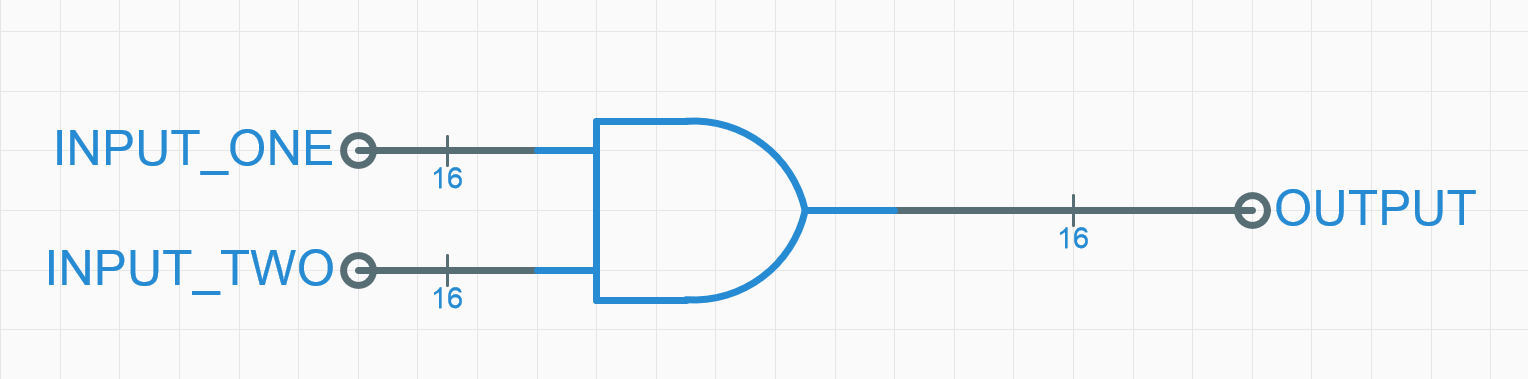
These two techniques can be combined, which will prove useful in the labs.
TESTING (not necessary to know unless you want to write your own tests)
The test aspect makes it easy to test the functionality of a module. Here's a test for an XOR circuit with inputs A and B, and output Z:
// Vol, Voh set voltages generated for input signals
// Vil, Vih set voltage thresholds for determining logic values
.thresholds Vol=0 Vil=0.1 Vih=0.9 Voh=1
// test actions are applied to named groups of signals.
// A signal can appear in more than one group. Order
// of groups and signals within each group determine
// order of values on each line of test values
.group inputs A B
.group outputs Z
// set type of simulation to be performed
// device -- transient simulation; components must be from from /analog
// gate -- gate-level simulation; components must be from /gates
.mode device
/* Tests are sequences of lines supplying test values; .cycle specifies
the sequence of actions that will be performed for each test. Available
actions are
assert group -- set values for signals in group with H,L test values
deassert group -- stop setting values for signals in group with H,L test values
sample group -- check values of signals in group with 0,1 test values
tran time -- run simulation for specified time interval
signal=val -- set signal to specified value
*/
.cycle assert inputs tran 9n sample outputs tran 1n
// the tests themselves -- one test per line
// to assert signal this cycle use 0,1; use Z or - if not to be asserted
// to sample signal this cycle use L,H; use - if not to be sampled
// whitespace can be used to improve readability, non-blank characters
// are associated, in order, with signals listed in .group above.
00 L
01 H
10 H
11 L
// (optional) produce plots showing the test inputs and/or outputs
.plot A
.plot B
.plot Z
The tests for a module can be run by clicking in the schematic toolbar.