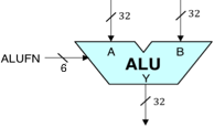
 The 32-bit ALU we will build will be a component in the Beta
processor we will address in subsequent laboratories. The logic
symbol for our ALU is shown to the right. It is a combinational
circuit taking two 32-bit data words A and B as inputs, and producing
a 32-bit output Y by performing a specified arithmetic or logical
function on the A and B inputs. The particular function to be
performed is specified by a 6-bit control input, FN, whose value
encodes the function according to the following table:
The 32-bit ALU we will build will be a component in the Beta
processor we will address in subsequent laboratories. The logic
symbol for our ALU is shown to the right. It is a combinational
circuit taking two 32-bit data words A and B as inputs, and producing
a 32-bit output Y by performing a specified arithmetic or logical
function on the A and B inputs. The particular function to be
performed is specified by a 6-bit control input, FN, whose value
encodes the function according to the following table:
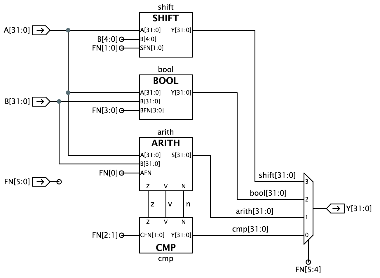
| FN[5:0] | Operation | Output value Y[31:0] |
|---|---|---|
| 00-011 | CMPEQ | \(Y = (A == B)\) |
| 00-101 | CMPLT | \(Y = (A \lt B)\) |
| 00-111 | CMPLE | \(Y = (A \le B)\) |
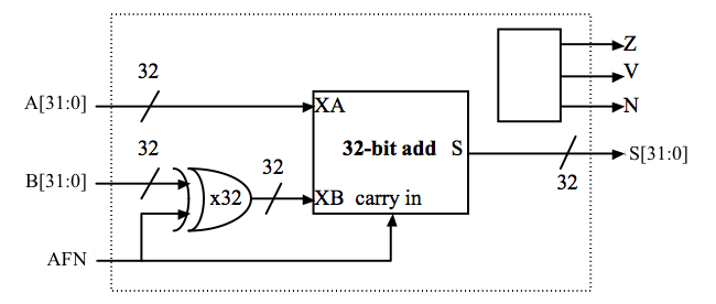
| 01---0 | 32-bit ADD | \(Y = A + B\) |
| 01---1 | 32-bit SUBTRACT | \(Y = A - B\) |
| 10abcd | Bit-wise Boolean | \(Y[i] = F_{abcd}(A[i],B[i])\) |
| 11--00 | Logical Shift left (SHL) | \(Y = A \lt\lt B\) |
| 11--01 | Logical Shift right (SHR) | \(Y = A \gt\gt B\) |
| 11--11 | Arithmetic Shift right (SRA) | \(Y = A \gt\gt B\) (sign extended) |
| Bi | Ai | Yi |
| 0 | 0 | d |
| 0 | 1 | c |
| 1 | 0 | b |
| 1 | 1 | a |
 Design the circuitry to implement the Boolean operations for
your ALU and use it to replace the jumper and wire that connects the Y[31:0]
output to ground.
Design the circuitry to implement the Boolean operations for
your ALU and use it to replace the jumper and wire that connects the Y[31:0]
output to ground.
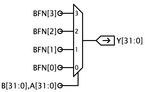
| Operation | BFN[3:0] |
|---|---|
| AND | 1000 |
| OR | 1110 |
| XOR | 0110 |
| "A" | 1010 |
| Comparison | Equation for LSB | CFN[1:0] |
|---|---|---|
| \(A = B\) | LSB = \(Z\) | 01 |
| \(A \lt B\) | LSB = \(N \oplus V\) | 10 |
| \(A \le B\) | LSB = \(Z + (N \oplus V)\) | 11 |
| Operation | SFN[1:0] |
|---|---|
| SHL (shift left) | 00 |
| SHR (shift right) | 01 |
| SRA (shift right with sign extension ) | 11 |